
OpenRISC 1000 (old)
Overview
To enable more developers of the OpenRISC processor and associated software to use a unified hardware platform a modular development board have been designed. Used together with the OpenRISC VMware image and a JTAG debug cable this provides a base for products based on the OpenRISC processor.
The following modules is included in the hardware platform
FPGA development board
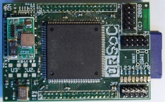
FPGA dev board ACTEL
Schematic ACTEL FPGA dev board, PDF
Resources on the board:
- ACTEL ProASIC3, A3P1000
- 1 Mbit SPI FLASH
- 32 Mbyte SDRAM
- SD FLASH connector
- 8 pin GPIO connector
- 8 LEDs
- 3 crystal oscillators, one with zero delay buffer with 5 outputs
- 10 pin header for debug (JTAG + UART)
- 10 pin header for FPGA configuration
- two 40 pin IO expansion board connectors
The FPGA board is 50 x 75 mm (2" x 3") . Along the longer sides there are 40 pin headers with 2 mm pitch with signals connected directly to the FPGA. The board can be used standalone, together with an expansion board or with application specific bards.
The FPGA board has enough memory resources to run a Linux kernel. There is a 32 Mbyte SDRAM and a SD connector enabling the usage of low price high capacity SD FLASH cards. This gives storage capability ranging up to gigabytes. Upon power-up the processor can copy an application from the SPI FLASH to SDRAM, for example a TFTP enabled boot loader.
The FPGA board has a 10 pin connector for easy debugging. When connected to the USB debug cable (described below) gives the developer both a UART to be used as a Linux console and JTAG debug capabilities on the processor.
The FPGA board has a 10 pin 2 mm pitch header used for power supply. Apply 3.3V and 1.5V (FPGA core supply) to this header. A local linear DC/DC converter is used to supply the FPGA built-in PLL. If used standalone there is a possibility to add a local DC/DC converter for the FPGA core as a small module.
These boards can optionally be populated with other FPGAs.
The following variants are possible:
| FPGA | System gates | Versa Tiles DFFs | 4608 bit blocks | RAM kbits | FLASH ROM bits | PLLs | Global nets | IO banks | IO SE/diff |
|---|---|---|---|---|---|---|---|---|---|
| A3P1000 | 1M | 24576 | 144 | 32 | 1024 | 1 | 18 | 4 | 147/65 |
| A3P1500E | 1.5M | 38400 | 270 | 60 | 1024 | 2 | 18 | 8 | 147/65 |
| A3P3000E | 3M | 75264 | 504 | 112 | 1024 | 6 | 18 | 8 | 147/65 |
Top
Expansion board
Expansion board Ethernet
Schematic ethernet expansion board, PDF
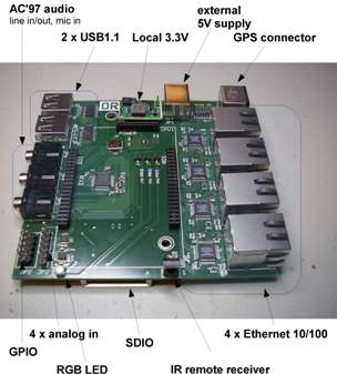
Resources on the board:
- 4 x Fast Ethernet PHY with RJ45 with magnetics and LED indicators
- 2 x USB 1.1 PHY with USB connector type A
- AC'97 audio codec with 3.5 mm jack for microphone in, line in and line out
- 4 channel analog to digital converter
- IR receiver for remote control
- RGB high intensity LED
- RS232 level shifter
- SD / SDIO connector
- 10 pin GPIO header
- USB type B connector for power supply
The focus for this expansion board is Ethernet connected devices. The board has four independent fast ethernet PHY devices each connected to a RJ45 with built-in magnetics and LED indicators. These PHY devices uses SMII communication to the MAC in the FPGA. This gives a very low pin count interface. As an option there is a possibility to connect a GPS to get a very precise time source to be used with NTP and/or IEEE1588.
This expansion board has two USB transceivers. These conforms with the "Serial Interface Engine". Both are connected to USB type A connector.
On the board there is also a 4 input analog to digital converter, a RGB high intensity LED, an IR receiver and some general purpose IO. There is also a connector for SD or SDIO cards.
On the boards there is also an AC'97 compatible audio codec. There is audio jacks for microphone input, line input and line output. The codec has built in functions for volume and balance and a connector for external power amp shutdown.
Possible usage of this expansion boards include
- Ethernet connected industrial IO module
- Ethernet connected audio devices
- Linux embedded system with USB hosts
Top
USB JTAG debug cable
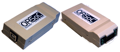
The USB connected JTAG debug cable enables easy connection to target with a console from a terminal emulator and debug support within GDB. The debug cable connects to a PC running a small JTAG proxy. GDB running on a computer can connect to the proxy via a TCP socket.
Top
Future work
Future work include design of new FPGA and expansion boards. Upcoming FPGA boards can be
used with existing expansion boards. This makes it easier to benefit from advantagesoffered by FPGA vendors. This also
makes it easy to adopt existing FPGA boards for new types of applications.
Possible resources on upcoming expansion boards
- Gigabit Ethernet
- VGA triple analog DAC or LVDS driver
- CAN
- USB2.0
- High speed analog to digital converters
Order information
To order boards contact ORSoC
Page maintainer(s)
This web page is maintained by
Top